Description
SiC Semiconductor Crystal Manufacturer | X-Z LAB
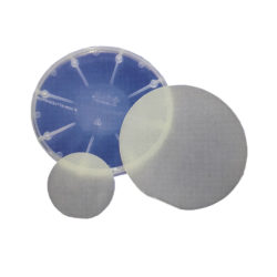
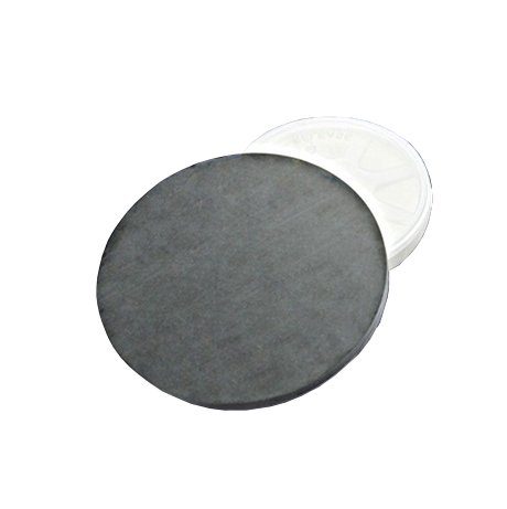
The SiC Semiconductor Crystal (Silicon Carbide) is a next-generation wide bandgap material designed for elite power electronics. Therefore, engineering teams choose this premium substrate because it provides exceptional thermal conductivity, high-saturation electron mobility, and excellent resistance to voltage. Consequently, these superior physical properties ensure that advanced electronic components operate reliably under extreme conditions.
Core Technical Advantages of SiC Semiconductor Crystal
-
Massive Energy Efficiency: Most importantly, SiC devices only have 50% energy loss compared with traditional Si devices, saving critical power.
-
High-Temperature Performance: The robust crystal lattice structure ensures stable operations within high-frequency, high-power, and high-temperature environments.
-
Radiation-Resistant Electronics: Furthermore, its high density and material purity deliver excellent shielding and durability against harsh radiation fields.
Advanced Industry Applications
Our specialized crystal growth processes ensure uniform electrical properties and flat wafer surfaces for industrial manufacturing. As a result, the SiC Semiconductor Crystal serves as the benchmark standard for modern green energy infrastructure and smart grid frameworks. Furthermore, its ultra-low power dissipation makes it highly effective for heavy industrial automation.
Main Applications of SiC Material
-
PV Inversion of Solar Energy: High-efficiency components for solar power inverters and renewable energy networks.
-
Heavy Electric Machinery: Industrial-grade power systems, electric vehicles, and heavy transit machinery infrastructure.
-
Power Switching: Next-generation power switching modules, smart grids, and high-frequency communication stations.
Why Choose X-Z LAB?
In conclusion, we control every phase of wafer production to provide reliable data and superior performance for your high-power electronic designs. If your project requires advanced radiation tracking or optical sensing, please explore our high-purity Photo Detector modules and complementary scintillation components. For global technical standards on silicon carbide substrates, you can consult established research guidelines provided by the IEEE Nuclear & Plasma Sciences Society.