Description
GaN Semiconductor Crystal Manufacturer | X-Z LAB
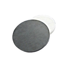
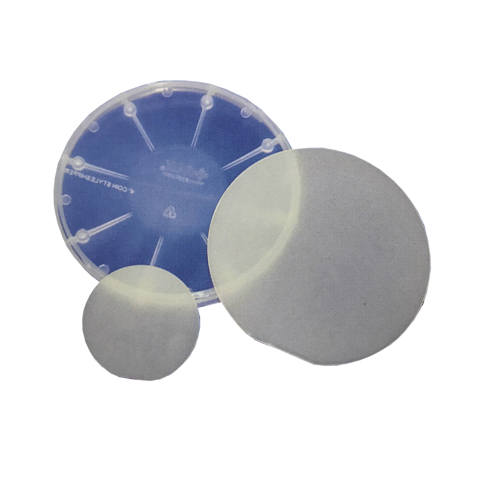
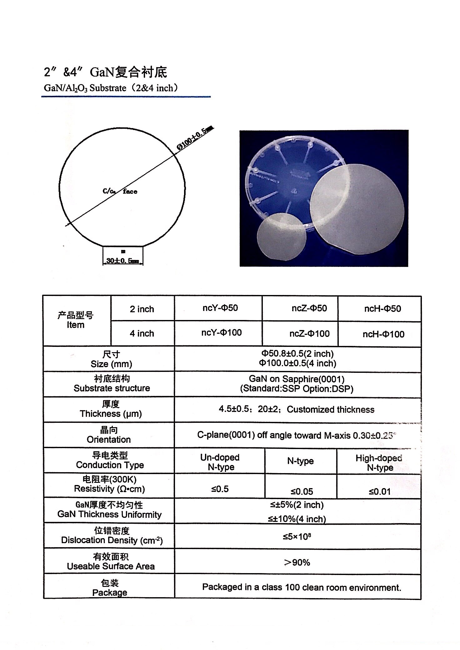
The GaN Semiconductor Crystal (Gallium Nitride) is a premier wide bandgap material engineered for next-generation optoelectronics and high-frequency power devices. Therefore, engineering teams choose this premium substrate because it provides an exceptionally high breakdown voltage, high-saturation electron velocity, and superior thermal conductivity. Consequently, these outstanding physical properties ensure that modern electronic components achieve maximum power density with minimal switching loss.
Core Technical Advantages of GaN Semiconductor Crystal
-
High Electron Mobility: Most importantly, GaN crystal devices support exceptionally high electron mobility, enabling ultra-fast switching frequencies.
-
Superior Power Density: The wide direct bandgap allows components to operate at much higher voltages and temperatures compared to traditional silicon.
-
Excellent Thermal Dissipation: Furthermore, its robust thermal properties ensure long-term stability and reliability in compact, high-power electronic subsystems worldwide.
Advanced Industry Applications
Our specialized crystal growth techniques deliver low defect density and precise wafer orientation required for critical commercial fabrication. As a result, the GaN Semiconductor Crystal serves as the benchmark standard for 5G/6G RF infrastructure, fast-charging power systems, and aerospace radar modules. Furthermore, its ultra-low bulk losses make it highly effective for cutting-edge solid-state lighting.
Main Applications of GaN Material
-
Optoelectronics and Lasers: High-efficiency blue and ultraviolet (UV) LEDs, laser diodes, and high-density optical storage systems.
-
RF and Microwave Devices: Advanced power amplifiers for military radar, satellite communication, and telecommunication infrastructure.
-
Power Conversion Electronics: Next-generation electric vehicle inverters, smart grid switches, and industrial power supply units.
Why Choose X-Z LAB?
In conclusion, we control every phase of manufacturing to provide reliable data and superior performance for your high-frequency electronic designs. If your project requires complementary optical materials or advanced radiation monitoring, please explore our high-purity Photo Detector modules and specialized scintillation components. For global technical standards on gallium nitride substrates, you can consult established research guidelines provided by the IEEE Nuclear & Plasma Sciences Society.